
Huawei just proposed replacing Moore's Law with a stopwatch, and Chinese chip stocks nearly hit their trading limits.
On May 25, 2026, at the IEEE ISCAS conference in Shanghai, He Tingbo, president of Huawei's semiconductor business department, delivered a keynote titled 'New Semiconductor Path in Practice'. She presented the Tau (τ) Scaling Law, a framework that abandons transistor size reduction in favor of minimizing signal propagation delay. Huawei claims it has secretly designed and mass-produced 381 chips over the last six years using these principles. The company projects that by 2031, its high-end chips will achieve a transistor density equivalent to a 14 Ångström (1.4 nm) process. The immediate consequence was visible on Chinese stock tickers: SMIC neared its trading limit, and Huahong Semiconductor surged nearly 20 percent. The U.S. sanctions strategy, fixated on controlling access to angstroms, just had a stopwatch thrown at it.
The Catalyst Was the Wall

Moore's Law is a dead end. The physical limits of 3nm and 2nm nodes are well documented. He Tingbo stated explicitly that Huawei hit this wall earlier than its peers due to "external restrictions." U.S. sanctions cut off access to ASML's extreme ultraviolet lithography machines, the essential tool for shrinking transistors. In the Global Times, she framed the sanctions as an accidental catalyst. The constraint forced a different question: if you cannot shrink the transistor, can you speed up the path the signal travels?
The 381 chips claim is the core evidence that this is not a laboratory theory. According to a report by Augmented Mind, Huawei says these chips were designed and mass-produced over six years. This number is contested. Western analysts cannot verify it independently. But the purpose of the claim is not transparency. It is scale. Huawei is signaling that a parallel, post-lithography supply chain is already operational.
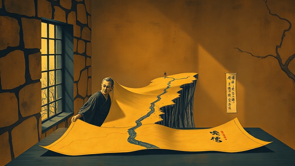
LogicFolding and the Shift from Space to Time
The enabling mechanism is LogicFolding. Huawei describes it as a vertically stacked, dual-layer 3D IC architecture that physically folds circuits to shorten the distance electrons must travel. The company claims a +55 percent effective transistor density improvement using this technique. The foundational paper, "A Time Scaling Theory for Multi-Layer Electronic Systems," was published by He Tingbo on ChinaXiv.org on the same day as the keynote.
The industry critique was immediate. Several observers, cited by Astro Awani, argued that reducing latency has always been a goal of semiconductor design. They note that the underlying techniques resemble existing work in 3D stacking and advanced packaging. The consensus dismissal is that Tau Scaling is just rebranded chiplet stacking.
This critique is technically accurate and strategically irrelevant. The innovation is the reframing. By shifting the metric from transistor size to signal delay, Huawei created a rhetorical and regulatory escape hatch. Sanctions control access to angstroms. They cannot control access to time. The Tau framework systematizes a post-sanctions design philosophy. It gives an entire ecosystem of Chinese chip designers a common target that does not require permission from ASML. The 381 chips claim, even if inflated, serves a single purpose: proving the framework works before anyone can call it vaporware.
The Geopolitical Bifurcation
Tau Scaling is a geopolitical manifesto. It declares the end of a single-track semiconductor industry governed by Western-controlled hardware. Tian Feng, director of Kuaisi Manxiang Research Institute, described it as a pivot "from a single track of process chasing to a dual track of process and design." This bifurcation is the real story.
Here is what I think happens next. Within 18 months, a major Western chip firm will publicly adopt time-domain scaling language to describe its own 3D stacking roadmap. Intel and AMD are both pushing vertical stacking architectures. They are already optimizing for signal path. They will not call it Tau Scaling. But they will describe their progress in terms of latency reduction and effective density, not just node names. This will inadvertently validate Huawei's framework.
The U.S. Commerce Department will face an absurd regulatory problem. Export controls are designed to restrict physical items: lithography machines, specific chip designs, certain materials. There is no legal framework to sanction "signal propagation optimization." A physics concept cannot be put on the Entity List. The U.S. will scramble to control the new enabling tools, likely 3D electronic design automation software and thermal dissipation technologies, but the conceptual frontier has already moved beyond its jurisdiction.
By 2030, the chip industry will be bifurcated. One track will continue the painful, expensive pursuit of 2nm and below, dominated by TSMC, Samsung, and ASML. The other track will pursue time-domain scaling, optimizing mature node processes through architecture, stacking, and signal-path engineering. This track will be dominated by Chinese firms who were locked out of the first one. The markets are already pricing this in. Chinese semiconductor equipment makers are becoming a decoupled asset class.
So What
For investors, the takeaway is structural decoupling. The Chinese chip sector is no longer a lagging play on Western node shrinks. It is betting on a different metric of progress. For tech leaders, the design toolchain is shifting. Mastery of 3D EDA software—the tools that model signal delay and thermal behavior across folded, multi-layer circuits—is the new bottleneck. For policymakers, the lesson is stark. Export controls on hardware are futile when the innovation frontier moves to architecture and time. You can sanction a machine. You cannot sanction a clock.
Moore's Law measured space. The West controlled the space. Tau measures time. China is claiming the clock.